�n�J
�U
���U
�U
�|������
�U
���b
�U
���V�ҵ{
�]�k�̤l
�U
�۸�X��
�U
�q�l��
�U
�ȪA����
�U
���z�����^�|��
�ѦW
�X����
�@��
isbn
�s��
5050�]�k���w
|
NG�ѫ�
|
��گū~�P�ҵ{
|
�u�f�q��
|
�R�E�^�����ֺ��
|
�L�B�z�����洹���զX�y���оǽd��(��CD)
�D
�b����s�{����(�Ĥ�
��Ǥp��
���
�U
�p��
�ӺЧ�
�]�g���
�U
��P����
�H�����{
�v�СB����
���|�B�H��B�v�a
���N�B����
�U
�q�v���@
�y�Ӿi��
�����B�O��
�Ʋz�B�ͬ��ʬ�
�Ш|�B�߲z�B�y��
�i�Dz�
�q���P����
�U
�y���u��
���x�B���Z
�U
�x�F�B�k��
�ѦҡB�ҸաB�Ь�ή�
��Ǥu�{
��ǡB�۵M
�U
�u�~�B�u�{
�a�x�ˤl
�a�x�B�ˤl�B�H��
�C�֦~�B����
���֤Ѧa
�ȹC�B�a��
�U
�T��
���e�B����
�U
�����
�b����s�{����(�ĥ|��)
�@�̡G
李克�@�B李克慧�B李明�f
�����G
�ѦҡE�ҸաE�Ь��
��
�j�M�ǰ|�Ь��
�X�����G
���عϮ�
�X������G2020/12/1
ISBN�G9789865035228
���y�s���Gkk0525940
���ơG360
�w���G
420
��
�u�f���G
88
��
370
��
�ѻ��Y�����ʡA�H�X������کw������
�q�ʫ�ߧY���z�i�f
�q�ʫ�ߧY���z�i�f�G�ثe�L�w�s�q,Ū�̤U�q��,�}�l�i�J�ծѵ{��,�@��ѼƬ���2-10�u�@��(���t�Ұ���)�C
���ʼƳ̧C�� 20 ���H�W
�����ơG
(�бN�ƹ����ܬP�P�B�i�����)
�ثe���������G
��r�s��
�ƻs�y�k
<a href='https://www.silkbook.com/book_detail.asp?goods_ser=kk0525940'>�b����s�{����(�ĥ|��)</a>
�Ϥ��s��
�ƻs�y�k
<a href='https://www.silkbook.com/book_detail.asp?goods_ser=kk0525940'><img src='https://www.silkbook.com/mall_image/bk/kk0525940.jpg' ALT='�b����s�{����(�ĥ|��)' height='120' width='90'></a>
��
��
���e²��
���y�ؿ�
�P������
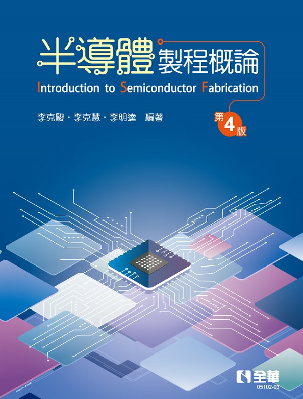
半導��s程概��(第四版) 內容簡介 全書分為五篇�A第一篇(1��3章)探�Q半導��材料之基本特性�A從矽半導��晶��結構�}始�A到半導��物理之物理概念�P��帶做完整的�ѻ��C第二篇(4��9章)��明積��q��使用的基礎元件�P先�i奈米元件�C第三篇(10��24章)��明積��q��的�s程�C第四篇(25��26章)��明積��q��的故�ٻP檢測�C第五篇(27��28章)��明積��q���s程潔淨控制�P安全�C全書�q用於大專�|校�q子�B�q機科系�u半導��s程�v或�u半導��s程技�N�v��程作為教材�C 本書特�� 1.深入淺出��明半導��元件物理和積��q��結構�B原理及�s程�C 2.從矽導��之物理概念�}始�A一直到半導��結構�B��帶作完整的�ѻ��A使Ū��學習到全盤知�ѡC 3.圖片清晰�A使Ū��一目瞭然更容易理�ѡC 4.�A用於大學�B科大�q子�B�q機系�u半導��s程�v或�u半導��s程技�N�v��程或相��業界人士及有����之Ū�̡C
�ؿ� �e�� �b����P�n��q�����o�i�v 0-1 �b���餧�t�_ (Semiconductor History) 0-2 �q���� (Transistor) 0-3 �n��q�� (Integrated Circuit) 0-4 �b����s�{ (Semiconductor Processes) �Ĥ@�g �b������ƻP���z ��1�� ���鵲�c�P���b���骫�z�S�� 1-1 ��l�ҫ��P�g���� (Atomic Model and Periodic) 1-2 ���鵲�c (Crystal Structure) 1-3 ����ɹq�� (Material Conductivity) 1-4 ���調�A��q�@�Ωw�� (Intrinsic Silicon, Mass-action Law) 1-5 �U����A�t���M���� (Dopant, n-type and p-type) ���D ��2�� �b�����a�P���l�ǿ� 2-1 ��a (Energy Band) 2-2 �q���Y�ƻP�����q�� (Resistivity and Sheet Resistance) 2-3 ���l�ǿ� (Carrier Transport) ���D ��3�� �ƦX���b���鴹�鵲�c�P���z�S�� 3-1 �ƦX���b���� (Compound Semiconductors) 3-2 �~���S���鵲�c�ί�a (Crystal Structure and Energy Band of Gallium Arsenide) 3-3 ����S���鵲�c�ί�a (Crystal Structure and Energy Band of Gallium Nitride) 3-4 �Ҥƪ����鵲�c�P��a (Crystal Structure and Energy Band of Silicon Carbide) 3-5 �U����A�t���M���� (Dopant, n-type and p-type) 3-6 �~���S�B����S�B�Ҥƪ��P����� (Comparison of GaAs�BGaN�BSiC and Si) ���D �ĤG�g �b���餸�� ��4�� �b�����¦���� 4-1 �G���� (Diode) 4-2 �����l�q���� (Bipolar Transistor) 4-3 ����b���Ĺq���� (Metal-Oxide-Semiconductor Field Effect Transistor) 4-4 ���ɪ���b���Ĺq���� (CMOS�AComplementary Metal-Oxide-Semiconductor Field-Effect Transistor) 4-5 �b����O���� (Semiconductor Memory) 4-5-1 �b���鴧�o�ʰO���� (Semiconductor Volatile Memory) 4-5-2 �b����D���o�ʰO���� (Semiconductor Nonvolatile Memory) 4-6 �q�� (Resistor) 4-7 �q�e (Capacitor) 4-8 �q�P (Inductor) ���D ��5�� ������a�ϻP�O�̯ඥ 5-1 �b���骬�A�K�� (Density of States) 5-2 �¥b����O�̤������ (Fermi Distribution Function of Intrinsic Semiconductor) 5-3 �U���b����O�̤������ (Fermi Distribution Function of Doped Semiconductors) 5-4 ������a�ϻP�O�̯ඥ (Junction Band Diagram and Fermi Level) ���D ��6�� �n��q���s�{�P�G�� 6-1 �����l�s�{�N (Bipolar Fabrication Technology) 6-2 ����b���Ĺq����s�{�N (MOSFET Fabrication Technology) 6-3 �q���P�n��q�� (Circuit and Integrated Circuit) 6-4 �]�p��h (Design Rules) 6-5 �G�� (Layout) ��7�� �b���餸���Y�p�ƻP���i�`�̤��� 7-1 ����b���Ĺq���餧�Y�p�� (Scaling of MOSFET) 7-2 �u�q�D���� (short-channel effects) 7-2-1 �t���M���� (velocity saturation) 7-2-2 �q�D�����ܮ��� (channel-length modulation) 7-2-3 ���{�ɹq�y���� (subthreshold current) 7-2-4 ������� (punch through) 7-2-5 CMOS��Ү��� (latch-up) 7-3 SOI���Ĺq���� (SOI-MOSFET) 7-4 �`���_�����Ĺq���� (FinFET) 7-5 �T���n��q�� (3 Dimensional IC) ���D ��8�� ���t�P���\�v�q���� 8-1 �~���S���b���Ĺq���� (GaAs Metal-Semiconductor Field Effect Transistor) 8-2 �~���S���q�l�E���v�q���� (GaAs High Electron Mobility Transistor) 8-3 ����S���q�l�E���v�q���� (GaN High Electron Mobility Transistor) 8-4 �Ҥƪ�����b���Ĺq���� (SiC Metal Oxide Semiconductor Field Effect Transistor) ���D ��9�� �b������q���� 9-1 �o���G���� (light emitting diode) 9-2 �p�g�G���� (Laser Diode) 9-3 ���P���� (Photodetector) 9-3-1 p-n���q�G���� (p-n Photodiode) 9-3-2 p-i-n���q�G���� (p-i-n Photodiode) 9-3-3 ���q�q���� (Phototransistor) 9-4 �Ӷ��q��(Solar Cell) 9-4-1 PERL�Ӷ��q�� (PERL Solar Cell) 9-4-2 ��ŤӶ��q�� (Tandem Solar Cell) 9-4-3 �D���Ӷ��q�� (Amorphous Solar Cell) 9-4-4 �E�� (Optical Concentration) ���D �ĤT�g �n��q���s�{�P�]�� ��10�� �����Τ��ͪ� 10-1 ��ưt�s (Starting Materials) 10-2 �����Υͪ� (Silicon Ingot Growth) 10-3 ����ͪ��ɺU���褧���G (Dopants Distribution in Crystal Growth) 10-4 ����ʳ��]Crystal Defects�^ ���D ��11�� �����ꤧ�s�@ 11-1 �����V�]Crystal Orientation�^ 11-2 ������V�B���ΩM�ߥ� (Orientation�BSawing and Polishing) 11-3 �Q�G�T����įq���R�]Benefit Analysis of 12 Inch wafer�^ ���D ��12�� �ƦX���b���鴹�Υͪ� 12-1 �~���S���Υͪ� (Gallium Arsenide Ingot Growth) 12-2 �ͪ� (Gallium Nitride Ingot Growth) 12-3 �Ҥƪ����Υͪ� (Silicon Carbide Ingot Growth) 12-3-1 ���Ū��z��ۨI�n�k (HTPVD) 12-3-2 ���ŤƾǮ�ۨI�n�k (HTCVD) ���D ��13�� ���U���ͪ� 13-1 �U�����]Epitaxial Layer�^ 13-2 ���U���ͪ��]Silicon Epiatxy�^ 13-3 ���U�����ͪ��{�ǡ]Growth Process of Si Epitaxial Layer�^ ���D ��14�� ���U���t�� 14-1 ���U���t�Ρ]Epitaxy Systems�^ 14-2 ���U���ͪ��t�Τ������]Evaluation of Epitaxial Systems�^ ���D ��15�� �ƦX���b����U������ 15-1 �~���S�U�������]GaAs Epitaxy�^ 15-1-1 �~���S�B�ƪ���۽U�� (Hydride Vapor Phase Epitaxy-HVPE) 15-1-2 �~���S�������ݤƾǮ�۽U�� 15-2 ����S�U���ͪ��]GaN Epitaxy�^ 15-2-1 ����S�B�ƪ���۽U�� (Hydride Vapor Phase Epitaxy-HVPE) 15-2-2 ����S�������ݤƾǮ�۽U�� 15-3 �Ҥƪ��U���ͪ��]SiC Epitaxy�^ ���D ��16�� ����ƽ��ͪ� 16-1 ������l�]Thermal Oxidation Furnace�^ 16-2 ����Ƶ{�ǡ]Oxidation Process�^ 16-3 �����ƻP���p�]Dry and Wet Oxidation and Thickness�^ 16-4 ����ƽ��p�����]Oxide Evaluation�^ 16-5 ����ƮɺU����l��������G (Redistribution of Dopant Atoms During Thermal Oxidation�^ ���D ��17�� ����ƽ��ͪ����� 17-1 �G��ƪ��P��ơ]Silicon Dioxide and Oxidation�^ 17-2 ��ƾ���]Oxidation Mechanism�^ 17-3 �W����Ƽh�]Ultra-Thin Oxide�^ 17-4 ��ƽ��~������]Oxide Quality Evaluation�^ 17-5 ��ƽ��~���i��k�]Improvement of Oxide Quality�^ ���D ��18�� �U���褧�X���ӤJ 18-1 �X������ (Concept of Diffusion) 18-2 �X���L�{ (Diffusion Process) 18-3 �X�������G���u (Distribution of Diffusion) ���D ��19�� �U���褧���l�G�� 19-1 ���l�G�� (Ion Implantation) 19-2 �h�� (Annealing) 19-3 ���l�G�ӦbCMOS�n��q���s�{�W������(Ion Implantation in CMOS IC Fabrication) 19-3-1 �վ�q�����{�ɹq�� (Adjustment of Transistor Threshold Voltage) 19-3-2 �Φ�N��P������ (Formation of N and P Wells) 19-3-3 �q���骺�j�� (Isolation) 19-3-4 �Φ��q���骺�����P�V�� (Formation of Source and Drain) 19-3-5 �Φ��C�U���@�ת��V�� (Lightly-Doped Drain Formation) 19-3-6 �U���ƴ��� (Poly-silicon Doping) 19-3-7 SOI����ͪ��ƻs (Preparation of SOI Wafer) 19-4 ���l�G�ӻs�{��� (Practices of Ion Implantation) 19-4-1 ����N�o (Wafer Cooling) 19-4-2 �������D (Resist Problems) 19-4-3 �q�����M (Charge Neutralization) 19-4-4 �L�лP�ìV (Dust and Contamination) ���D ��20�� �L�v�N 20-1 �L�v�k��N (Lithography) 20-2 ���n���s�@ (Fabrication of Mask) 20-3 ���L�v�N (photolithography) 20-4 ���ѪR�W�j�L�v�N (Resolution Enhancement Techniques) 20-5 �L�v�N������ (Photolithographic sources) 20-5-1 �q�l���L�v�n���t�� (Electron Beam Lithography) 20-5-2 ���`���~���L�v�n���t�� (Extreme Ultraviolet Lithography) ���D ��21�� �k��N 21-1 ��k�� (Wet Etching) 21-1-1 ����k�� (Si Wet Etching) 21-1-2 �ƦX���b������k�� (Compound Semiconductor Wet Etching) 21-2 ���k�� (Dry Etching) 21-2-1 �q�e���X���q�k��� (Capacitively Coupled Plasma etcher) 21-2-2 �������l�k��� (RIE-Reactive Ion Etcher) 21-2-3 �������U�D���V�ʻk�� (Anisotropic Etching Assisted by Sidewall Mechanism) 21-2-4 �q�P���X���q�k��� (Inductively Coupled Plasma Etcher-ICP) 21-2-5 ���ݹq�k��� (Remote Plasma Etcher) 21-2-6 �ƦX���b���鰮�k�� (Compound Semiconductor Dry Etching) 21-2-7 ��l�h�k��N (Atomic Layer Etching) 21-2-8 �E�J���l�� (Focused Ion Beam, FIB) 21-2-9 �ƾǾ���ߥ� (Chemical-mechanical polishing, CMP) ���D ��22�� �ƾǮ�ۨI�n 22-1 �ƾǮ�ۨI�n���� (Introduction of CVD) 22-2 �ƾǮ�ۨI�n�y�{ (CVD Procedures) 22-3 �C���ƾǮ�ۨI�n (Low Pressure CVD - LPCVD) 22-4 �q�ߤƾǮ�ۨI�n (Plasma CVD - PCVD) 22-5 ���ӤƾǮ�ۨI�n (Photo-CVD) 22-6 ��l�h�I�n (Atomic Layer Deposition) 22-7 �G�ۨI�n�k (Liquid Phase Deposition) ���D ��23�� ���ݱ�IJ�P�I�n 23-1 ���ݤƤ��n�D (Metallization Requirements) 23-2 �u�ŨI�n (Vacuum Deposition) 23-3 �I�n�N (Deposition Techniques) 23-4 �u�ŨI�n�{�� (Vacuum Deposition Procedure) 23-5 �X��/�h�� (Alloy/Annealing) 23-6 ���ݪ��ƪ� (Silicide) 23-6-1 �U���h���� (Doped Polysilicon) 23-6-2 ���ݪ��ƪ��P�h�����ƪ� (Silicide and Polycide) 23-7 �ɻs�{�N (Copper Processes) ���D ��24�� �n��q���ʸ� 24-1 �n��q���ʸ� (IC Package) 24-1-1 �n��q�����b���餸�Ī��D�] (IC Failure Analysis) 24-1-2 �ʸ˪��\�� (Function of Packaging) 24-1-3 �n��q���ʸ˧��ƪ��n�D (Material Requirements) 24-2 �ʸˤ��� (Classification) 24-3 �ʸˬy�{ (Packaging Flow Chart) 24-3-1 �I����i (Back-Side Grinding) 24-3-2 �����z�� (Chip Sorting) 24-3-3 ������� ( Sawing) 24-3-4 �Z�� (Die Attaching) 24-3-5 �Z�u (Wire Bonding) 24-3-6 �ʽ� (Molding) 24-3-7 �q�� (Solder Plating) 24-3-8 �s�}���� (Forming) 24-3-9 �̫���� (Final Testing) 24-3-10 ���] (Packing) 24-4 �T���ʸ� (3 Dimensional Package) ���D �ĥ|�g �n��q���G�ٻP�˴� ��25�� �i�a�P�\����˴� 25-1 �i�a�װ��� (Basic Idea of Reliability) 25-2 �i�a���˴� (Reliability Testing) 25-3 �G�ټҫ� (Failure Models) 25-3-1 �G�٥����ةR (Mean-time-to-failure�AMTTF) 25-3-2 �����G�ٶ��j�ɶ� (Mean-Time-Between-Failure, MTBF) 25-4 �q�Ϥz�Z (EMI) 25-5 �R�q���� (ESD) 25-6 �\����˴� (Function Testing) 25-6-1 �i�˴��]�p (Design for Testability) 25-6-2 ���ئ��ۧ��˴� (Built-in Self-Test, BIST) 25-6-3 �i���@ (Repairable) ���D ��26�� ���ƯS���˴� 26-1 �����κA���R���� (Surface Morphology Analysis Instruments) 26-1-1 ������L�� (Optical Microscope-OM) 26-1-2 ���y���q�l��L�� (Scanning Electron Microscopy- SEM) 26-1-3 ��l�O��L�� (Atomic Force Microscopy-AFM) 26-2 ���鵲�c���R���� (Crystal Structure Analysis Instruments) 26-2-1 X��¶�g���� (X-ray Diffraction Spectrum) 26-2-2 ��z���q�l��L�� (Tunneling Electron Microscopy-TEM) 26-3 �զ����R���� (Composition Analysis Instruments) 26-3-1 �G�����l���л� (Secondary Ion Mass Spectrometer-SIMS) 26-3-2 �ť߸��ഫ���~���W�л� (Fourier Transform Infrared spectroscopy: FTIR) 26-3-3 �ڳǹq�l���л� (Auger Electron Spectroscopy-AES) 26-3-4 X�g�u���q�l���л� (X-Ray Photoelectron Spectroscopy-XPS)�ΤƾǤ��R�q�l���� (Electron Spectrometry for Chemical Analysis-ESCA) 26-3-5 �ҥ��л� (Raman Spectroscopy) 26-3-6 ���E���л� (Photoluminescence Spectroscopy-PL) ���D �Ĥ��g �s�{��b����P�w�� ��27�� �s�{��b����P�w��(�@) 27-1 ��b�{�� (Cleaning Procedures) 27-2 �� (Water) 27-3 �Ů�/�L�Ы� (Air/Clean Room) 27-4 �H�� (Personnel) 27-5 �ƾ��ī~ (Chemicals) 27-6 ���� (Gases) ���D ��28�� �s�{��b����P�w��(�G) 28-1 ������~ (High Pressure Cylinder) 28-1-1 ������~���ϥ� (Usage of High Pressure Cylinder) 28-1-2 ������~���J�s (Storage of High Pressure Cylinder) 28-2 ���O�ո`�� (Pressure Regulator) 28-3 �j�b (Blow Up) 28-4 ���|���� (Leak Check) 28-5 �]�ƤW���`�N�ƶ� (Equipment Check) 28-6 �o�𤧱Ʃ� (Exhaust) 28-6-1 ����Ʃ� (Gases Exhaust) 28-6-2 �Ʃ���骺���`�B�z (Toxic Gases Treatment) 28-7 �������`�N�ƶ� (Emergency) 28-7-1 ���|����ɪ����B�m (Emergency Treatment of Gases Leak) 28-7-2 �o�ͤ�ĵ�ɪ����B�m (Emergency Treatment of Fire Alarm) 28-7-3 ���r�ɪ����B�m (Emergency Treatment of Poisoning) 28-7-4 �w�� (Precaution) ���D
�s�s���Ҭr����(�ĤG
�ͬ����(�Ĥ���)
���~���@�z�N(�ĤQ
Java�{���]�p�J��
�{�N�ӥέ^��w�w�ѫH
�������(�ĤG��)
�Ů𦾬V����G�z�פ�
������(�Ĥ���
�s�s�����Ū(�ĥ|��
���@�z���`�Ʋߢw��
���F�O�ٱz���v�q�A�s���������ѩ����ʶR���ӫ~���ɦ���f�C�Ѫ�Ų����]�t�Ұ���^�C�h�^���ӫ~������Ų������H�^�]�H�l�W�Φ����p���̡^�A�B�ӫ~�����O���s���A�P����]��(�ӫ~�B����B���~�]�ˡB�H�f���B�ث~��)�A�_�h���������h�f�C